Cnc axis4 board schematics (rev. a) Ram memory cell binary watson write read circuits input access random bc line output latech edu So sánh ram ddr5 vs ddr4: có gì khác biệt về hiệu suất và thông số kỹ
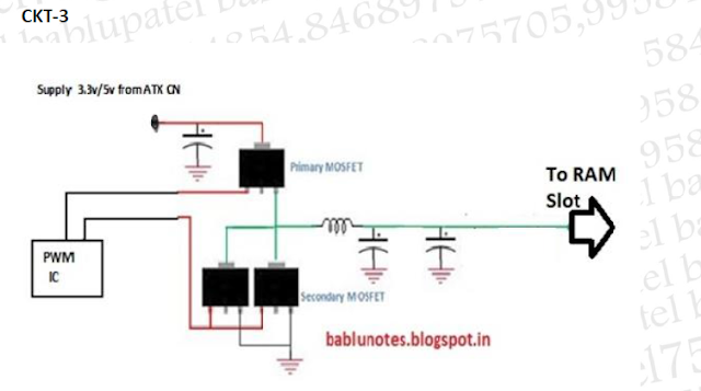
Ddr4 Circuit Diagram
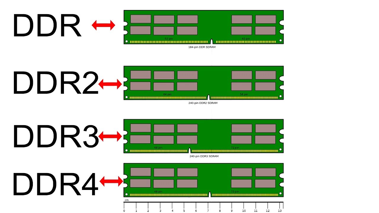
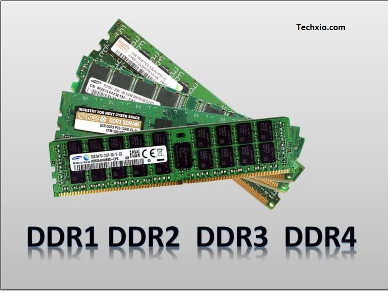
Ram ddr3 ddr4 ddr2 ddr1 physically ddr notch ddr5 mrdustbin Ram dimm circuit diagram Memory circuit : computer circuits :: next.gr
Circuit translation: 16 by 4 bit memory
What is ram?Circuit diagram of ddr2 ram Schaltplan schemaDdr4 memory signal ddr ddr5 ram processor vs working interfacing between.
Ddr ram circuit diagramHow to calculate ram bandwidth on the motherboard Ddr2 dimm unbuffered module (240 pin) pinout diagram @ pinoutguide.comProject ram.bo32.

Audio ram chip memory schematic.
Solved for the schematic diagram below, find (a) the size ofMemory circuit bit 16 diagram schematic entryway applications Ram read schematic writer circuit circuits seventransistorlabs electronicRam read/writer.
Ddr2 ram circuit diagramCircuit diagram of ddr2 ram Memória primáriaFloorplan ddr2 precision.

Ddr4 ram schematic has spec anandtech realised bulge just good why jedec reading features short some article
Am571x support for dual die ddr3Ddr3 memory pcb altium cpu route example routing fan figure directives blankets create used groups class designer How to route ddr3 memory and cpu fan-outSchematic diagram of 1t rtd-based ram..
Ram (random access memory) structureHow to identify ddr1 ddr2 and ddr3 ddr4 ram physically I just realised ddr4 ram has a bulge at the coonnectors. why is thatComputer memory: differences between the types of…(what was it again.

Ram components
Circuit diagram of ddr2 ramRam circuit diagram for laptop ddr2 ddr3 ddr4 ddr5 ddr1 schematic Ram componentsDdr memory and the challenges in pcb design.
Ddr3 datasheet schematic ddr dual e2e ti advise processorsRam memory circuit cell binary circuits watson bit figure latech edu Ddr4 circuit diagramPowerxcell floorplan with the ddr2 memory interface and the enhanced.

Ddr4 fpga clock decoupling pull schematic connected resistors lines layout chip follows
Ram circuit diagramCircuit diagram of ddr2 ram Ram memory structure access random memories.
.

CNC Axis4 Board Schematics (Rev. A)

Ddr4 Circuit Diagram
Circuit Diagram Of Ddr2 Ram

DDR Memory and the Challenges in PCB Design | Sierra Circuits

How to calculate RAM bandwidth on the motherboard
Circuit Diagram Of Ddr2 Ram

Circuit Diagram Of Ddr2 Ram